
Our current research efforts, in short:
I. Photo-thermoelectric effects in semiconductors
Supported by NSF CAREER award 2024-2029, this study will allow better understanding of materials' photo-thermoelectric response in general, in order to design better optical sensors.
Thermoelectric effects are most discussed in systems in thermodynamic equilibrium, under a temperature gradient; photo-electric effects are induced by photon excitation of semiconductors, creating non-equilibrium conditions at constant temperatures. At their interface photo-thermoelectric effects are observed, which are transport processes in semiconductors with excited carrier distributions and under temperature gradients. Better understanding of photo-thermoelectric effects is needed, which provides insights to fundamental material properties, and also has the potential for improved properties of (thin film) thermoelectric devices for energy conversion or sensing applications.
At first glance, the photo-thermoelectric effects differ from conventional thermoelectric effects due to the two separate ‘Fermi distribution’ of electrons and holes in the same material, which can be modeled given basic material parameters. However, the actual phenomenon is much richer than that and many other factors could play a role: temperature coefficient of photovoltaic effects (both from Schottky barriers and lateral diffusion), hot carriers, defects and traps, etc.
We take photo-Seebeck coefficient, photo-Hall effect and photoconductivity as a whole to sort through influences from different factors, as well as understanding the generality and differences in samples with different doping, and across different material systems. Some exciting development planned include transient photocurrent test, thermoelectric spectroscopy for defect study, and scanning photo-thermoelectric current microscopy.


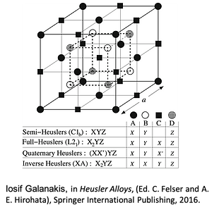
II. Defect and disorder in Spin Gapless Semiconducting Heusler compounds
As part of a team supported by a NSF FuSe (Future of Semiconductors) award 2023-2026, we are looking into the defects and disorders in the Heusler compound of Mn2CoAl. This effort will allow us to better understand how defects and disorders are affected by composition and heat treatment, and how they in turn affect the materials magneto-transport properties and its potential in a spintronic readout device.
Heusler compounds are a big family of intermetallics. A Heusler unit cell is made of several intercalating FCC sub-lattices, resulting in both tetragonal and octahedral bonds. Heusler compounds have wide applications as ferromagnets, shape-memory alloys, spintronic materials, and thermoelectric materials. Many Heusler compounds have spin-specific band structures: so-called half-metallicity and spin gapless semiconductivity, So the material behaves like a metal (or a gapless semi-metal) for electrons of one spin, and an (intrinsic) semiconductor for those with the opposite spin. Even in regular semiconducting states, Heusler compounds are quite different from conventional semiconductors because their conduction and valence bands are both made up of d states. For instance, the carrier densities are much higher, the temperature dependence of mobilities are much weaker.
Our current research aims at materials with better performance as thermoelectrics and spin gapless semiconductors. Heusler compounds tend to have significant amount of intrinsic defects. These structural defects are unwanted for many applications, yet they are hard to avoid, sometimes due to thermodynamics, sometimes due to the difficulty navigating through a complex phase field. We believe it is important to better understand the phase diagrams. From there we learn the dominant defects at different conditions, and how do they affect the electronic structure. Lastly we look for strategies to optimize the electronic structure and thus properties. Our primary tools include Thermo- and magneto-electric property measurements and transport property modeling.


III. Solution processed nano-thermoelectrics
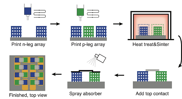
Researchers love nano-materials for thermoelectrics for various reasons. For us we see two merits that one can't get with bulk materials. The first is the superior morphology and size control from solution processing, which provided great convenience when it comes to the printing of such materials for conventional and unconventional devices. This capability is critical for the realization of segmented device design via additive manufacturing (see for example the figure below) for alternative TECs, as well as other devices beyond that.
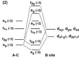
The second, which is perhaps more interesting, is that nano-materials can potentially provide a means of band engineering for thermoelectric materials to achieve high zTs. Supported by a NSF MPS-LEAP award (2022-2024), we are studying hydrothermally synthesized Te nanosheets to explore this strategy. To understand the effectiveness of band engineering for thermoelectrics, consider the fact that all known good thermoelectrics have such in common, that their band structure contain multiple degenerate carrier pockets and their Fermi surface are very complex (see figure below). The goal of band engineering is to induce such kind of complex Fermi surfaces.

IV. Ductile inorganic semiconductors
Common intuition tells us that metals are ductile and semiconductors are brittle. However, some inorganic semiconductors, such as a-Ag2S, have excellent ductility that stands out even among metals. We believe this opens an avenue toward flexible and robust electronic devices for wearable applications, using cost-effective metallurgical processes, such as rolling, weaving, or stamping, rather than traditional semiconductor fabrication. We are exploring reliable device design and fabrication of light sensors and alike. A related effort is to understand what impacts the severe plastic deformations make on carrier density, mobility, deep defect states, as well as ionic conductivity.

II. Design of new thermoelectric devices
Essentially all thermoelectric devices available on market is made of some alloys of Bi0.5Sb1.5Te3 and Bi2Te2.7Se0.3. These materials are expensive and fragile. It would be great if we have alternatives made with, for instance, deformable materials so that devices are robust under impact. The wearable electronics are such kind of application. Often the high performance in current devices is arguably not as important.
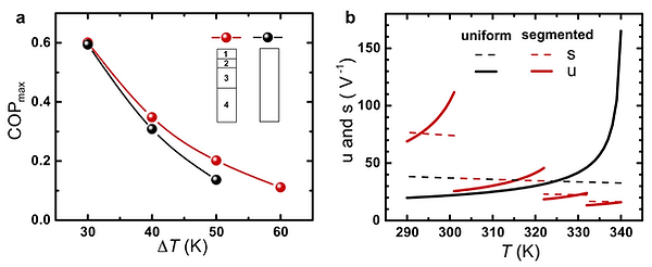
Nonetheless, since deformable thermoelectric materials known today have much lower zTs than currently used materials, without rational device design the performance of such devices will likely fall short of what is practical. We looked into this issue, first considering material pairing principles. This result is now published in Materials Today Physics.

To use what we have today to their full potential, we are also looking into devices made with more than two materials, similar to the functional graded design (yet fundamentally different). We believe this design could allow different parts of a device to operate closer to their optimum conditions such that the device as a whole could perform better.
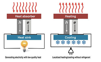
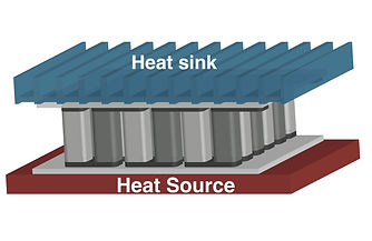
The building block (left) of a thermoelectric device is a "thermocouple": a pair of a n-type and a p-type semiconductor in a "Pi" shaped configuration. Under a temperature gradient, the thermally driven electrons and holes in each material provide electrical power. This give rise to the first application of generating power. In reverse, when power is supplied and electrons and holes flow through the "thermocouple", the generation/annihilation of electrons and holes cools down/heats up on one side of the device, giving rise to the second application of heating and cooling without refrigerant. In practice, several tens of such "thermocouples" are positioned in pattern, bond with proper contact as well as a heat absorber and a heat sink. This assembly is a module (right), most applications use multiple modules altogether.
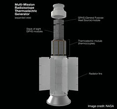
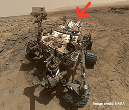
Thermoelectric technology found its most successful application in space missions, where solar energy is not sufficient. NASA's Mars Laboratory "Curiosity" landed on Mars in 2012 (left), is powered by a radioisotope heated thermoelectric generator with 135 Watt output, the Multi-Mission Radioisotope Thermoelectric Generator (MMRTG, right). In this selfie of Curiosity taken in 2017, the MMRTG can be clearly seen at the back of the rover (right arrow).
In a broader context, one can get a large piece of transport properties of a semiconductor from answers to the questions above. This information is relevant to most applications of semiconductors. For example, building a IC circuit requires very exact information about mobilities and concentration of carriers under different conditions. Transparent semiconductors, an essential part in all the LCD/LED/OLED displays, demand low cost, large band-gap semiconductors with very high carrier concentration and high mobility. Optoelectronics such as photovoltaics and light emitters should be materials with proper band gaps, low intrinsic carrier concentration, and high carrier mobilities. There are also applications with low mobility semiconductors, such as sensors or electrodes. In this case even though charge transport details are not as critical, a better understanding is still beneficial for material design strategies.
A less noticed complexity with semiconductors is that, they could be good for different applications under different doping levels. Silicon for example, is a great semiconductor for wafers/substrates, where it has very few free carriers (~10^12 cm-3) and is semi-insulating. When used for photovoltaics, it has higher carrier concentrations (~10^16 cm-3). When used as conduction channels in transistors, it is doped with way more carriers (~10^19 cm-3). Finally, it forms one of the most successful thermoelectric compounds (Si-Ge alloy) with even higher carrier concentrations (>10^20 cm-3). The same is true for III-V semiconductors for their applications ranging from spintronics, to light emitters, to heterojunction devices. In another word, a sample tested great for one application is probably not good for another, for the same reason, a compound tested poorly for one application is not necessarily poor after being optimized. A semiconductor compound has to be carefully “tuned” for each different application.
The “tuning” usually start with controlling free carrier type and concentration. What guide that “tuning” process, is the understanding of transport process in that compound, i.e., answers to the questions above.
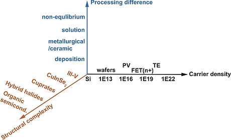
The material exploration involving semiconductors is a problem on three different dimensions: composition, doping, and processing.
Understanding the transport, and answering the questions listed in the beginning requires reliable measurement and matching result with Boltzmann transport modeling. This is one focus of our research.
Controlling free carrier type and concentration by doping, is the other focus of ours. Even though the principle is quite straightforward, doping of a semiconductor is often difficult. Most of the III-V semiconductors can only be doped either n- or p-type, which is a significant obstacle in their application in integrated circuits since a standard CMOS unit can’t be made. In thermoelectrics, “dope-ability” has limited many materials systems from achieving anticipated performance. It is even more challenging to dope many emergent semiconductors such as polymers, quantum dots, solution-processed materials.

In our research, "doping" refers to this classic picture of atomic substitution by hetero-valent atoms. Si is used as an example.
Doping is a center piece for semiconductor research as well. It is through the transport measurement of samples with widely different carrier concentrations that we get insights on the band structure, or the significance of different carrier scattering mechanisms. No other technique could provide such information.
Computational methods have made great progress and have been facilitating semiconductor research dramatically. Both the band structures and defect formation enthalpies can now be computed. However, for accurate information on band gap, effective mass, or phase diagrams, the experimental methods are still the only way to know for sure. There has not been a way to compute/predict the mobility of carriers in a compound, or the doping range of a certain dopant.
Doping is the theme connecting most of our research efforts
To a great extend, the research on thermoelectrics is a game of doping, where careful optimization of carrier concentration is essential for achieving the best thermoelectric performance for a semiconductor. Heng dealt with this challenge throughout his PhD research. We will be constantly in this game as well. Besides, there are a few occasions we need to think outside of conventional doping with hetero-valent substitutions: first, we want more than just tuning the carrier concentration. or second, doping is not applicable/successful.
Resonant dopants (ongoing effort)
A good example for the first occasion is the resonant dopants. It is seen in IV-VI semiconductors like PbTe, PbSe and SnTe, that when certain non-magnetic and substitutional dopants are used, the charge transport of that compound behave differently from the general trend with the majority of “regular” dopants. Such difference can’t be explained by changing of carrier chemical potential, effective mass, or relative configuration of band structures. Rather, it is seen as the result of interaction between band-like extended states from the periodic lattice and defect-like localized levels from localized dopants. resonant dopants could have a positive impact on thermoelectric properties of the semiconductor. Its impact on other applications has yet to be determined.
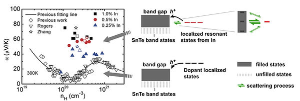
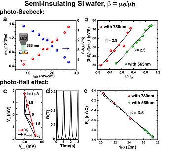
In dopant forms resonant states in SnTe. In contrast with other regular dopants, it led to drastically different transport behaviors. As shown in the data plot [from this article] the Seebeck coefficient is higher given the same Hall carrier concentration, which is desired for thermoelectrics. On the energy scale, the difference between In dopants and regular ones are illustrated in the right part of the figure. In the regular dopant case the picture is same as in textbooks: localized states from dopants are at a slightly lower energy (for holes) than the valence band edge. They are thermally excited, donating holes to SnTe band as charge carriers. There is no scattering afterward between dopant states and the band states. In the resonant dopant case as one way to explain this, localized In states are found at a higher energy than the valence band edge. holes are donated to SnTe band even without excitation. Meanwhile, carriers from the band scatter to and from In localized states. This scattering is strongest between states same in energy, and decreases and the energy difference increases, giving its name "resonant scattering".
Currently, there isn't a theory good enough to quantitatively describe the influence of resonant dopants on transport properties. Heng had studied resonant dopants of Tl in PbSe, and In in SnTe. Currently, based on those experiences, we are trying to find a proper treatment under the Boltzmann transport and relaxation time approximation to better explain, then predict, the unique transport behaviors in such systems.
Doping by inert secondary phases
In a recent research in collaboration with researchers from Tsinghua University and Temple University, Heng found the semiconductor of PbSe can be doped by chemically inert secondary particles such as Si, SiC, even diamond. No hetero-valent dopants were present, yet the carrier concentration clearly exceeded what is achievable without extrinsic dopants. The only plausible explanation is electronically active defects accumulated at the interfaces. This discovery inspired us to think out of the box when regular substitutional doping is not an option. We would like to explore applicability of this in other compounds, and eventually use it as a strategy to dope semiconductors that can’t be doped otherwise.
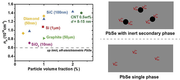
Taken from this work, the data plot to the left showed the Hall carrier concentration in PbSe with different types of secondary phase particles. All of these particles are chemically inert. No regular dopants were introduced. the dashed line denotes the upper limit carrier concentration in PbSe without of use of an foreign dopant. This result was explained with higher concentration of intrinsic defects (Se vacancies illustrated as a possible case) at particle-matrix interface generated by non-equilibrium synthesis.
Doping of solution processed semiconductors
Today, making semiconductor devices involves high temperature crystal growth, vacuum deposition, and lithography. Other functional semiconductors in labs are made through other high-temperature, high-energy, metallurgy or ceramic based processes. Solution processed semiconductor could drastically change this picture. Imagine crystals or thin films can be grown from solutions like sugar, and semiconductors can be applied like paints to places needed, or even an entire device can be “printed” with additive manufacturing. This could revolutionize where electronics are used or how they are used.
There are many obstacles on the way there. One of them is: how can we dope them. Today’s semiconductors are doped primarily using three different methods 1) addition and reaction, 2) ion implantation, and 3) diffusion. None of them are readily applicable to solution processed semiconductors. The existence of solvent phase, the lack of a dopant activation process, and the availability of elements only in form of ions, these all set limitations on doping of solution processed semiconductors, which is probably why successful doping examples are so rare.
Doping with other sources of excitation (see current research topic I)
Free carriers in a semiconductor can be generated by means other than dopants. These include photons (lights), heat, and electric field. None of these provide persistent free carriers, but still they have their unique value for research. Why?
There is always a strong initiative to look for better, new semiconductors for different applications, such as thermoelectrics. For some applications, high throughput material discovery by first principle calculation has been employed with success. Nonetheless, so far it is still daunting to get transport properties ( mobilities and carrier densities) of a compound from calculation. Moreover, predicting how and how much different compounds can be doped is also a grand challenge. We have to rely on experiments.
To study the transport of a semiconductor, we need to measure multiple samples with widely different carrier concentrations. This is a nontrivial task: finding suitable dopant, optimizing the synthesis, assuring consistently high quality among all samples, etc. In the end, it takes too much work to “screen” new materials and experimentalists can’t keep up with the demand.
We hope we can help accelerate this by not actually doping a compound with dopants, but instead exciting free carriers just for measurements. The change of carrier concentration is achieved by changing excitation (such as incident light) intensity. Transport properties including Seebeck coefficient, conductivity, Hall coefficient, and magnetoresistance are measured on a single sample under different conditions. Multiple-band Boltzmann transport analysis is then used to solve for parameters including concentrations and mobilities of electrons and holes, their effective masses or scattering mechanisms.
What are we generally interested in, and why are they important:
We are interested in studying charge transport, as well as heat transport in semiconductors. For a great part of our research, we ask ourselves (and try to answer) the following questions:
-
What is the band structure of this compound of XXX?
-
What is the intrinsic free carrier type and concentration?
-
What are the effective masses and mobilities of its electrons and holes?
-
How do all the above change with temperature?
-
How do they change with composition, and doping levels.
These questions are important for applications such as thermoelectric conversions. In this application, a type of heavily doped semiconductors form the centerpiece of a solid-state device, which generate electric power under a temperature gradient, or heat up/cool down a local area when power is supplied.